- 您现在的位置:买卖IC网 > Sheet目录510 > SI4731-D50-GM (Silicon Laboratories Inc)IC RADIO RECEIVER AM/FM 20-QFN
�� �
�
�Si4730/31-D50�
�4.17.� Control� Interface�
�A� serial� port� slave� interface� is� provided,� which� allows� an�
�external� controller� to� send� commands� to� the� Si4730/31�
�and� receive� responses� from� the� device.� The� serial� port�
�can� operate� in� two� bus� modes:� 2-wire� mode� and� 3-wire�
�mode.� The� Si4730/31� selects� the� bus� mode� by� sampling�
�the� state� of� the� GPO1� and� GPO2� pins� on� the� rising�
�edge� of� RST.� The� GPO1� pin� includes� an� internal� pull-up�
�resistor,� which� is� connected� while� RST� is� low,� and� the�
�GPO2� pin� includes� an� internal� pull-down� resistor,� which�
�is� connected� while� RST� is� low.� Therefore,� it� is� only�
�necessary� for� the� user� to� actively� drive� pins� which� differ�
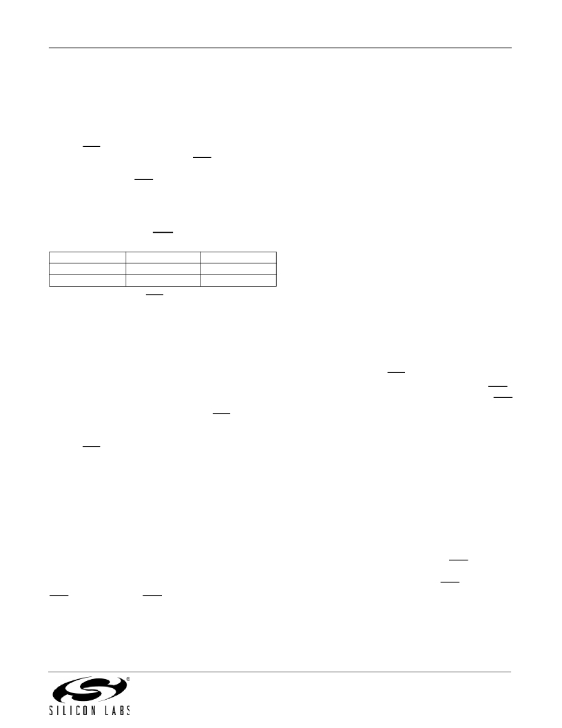
�from� these� states.� See� Table� 13.�
�Table� 13.� Bus� Mode� Select� on� Rising� Edge� of�
�RST�
�Bus� Mode� GPO1� GPO2�
�2-Wire� 1� 0�
�3-Wire� 0� (must� drive)� 0�
�After� the� rising� edge� of� RST,� the� pins� GPO1� and� GPO2�
�are� used� as� general� purpose� output� (O)� pins,� as�
�described� in� Section� “4.18.� GPO� Outputs”.� In� any� bus�
�mode,� commands� may� only� be� sent� after� V� IO� and� V� DD�
�supplies� are� applied.�
�In� any� bus� mode,� before� sending� a� command� or� reading�
�a� response,� the� user� must� first� read� the� status� byte� to�
�ensure� that� the� device� is� ready� (CTS� bit� is� high).�
�4.17.1.� 2-Wire� Control� Interface� Mode�
�When� selecting� 2-wire� mode,� the� user� must� ensure� that�
�SCLK� is� high� during� the� rising� edge� of� RST,� and� stays�
�high� until� after� the� first� start� condition.� Also,� a� start�
�condition� must� not� occur� within� 300� ns� before� the� rising�
�edge� of� RST.�
�The� 2-wire� bus� mode� uses� only� the� SCLK� and� SDIO�
�pins� for� signaling.� A� transaction� begins� with� the� START�
�condition,� which� occurs� when� SDIO� falls� while� SCLK� is�
�high.� Next,� the� user� drives� an� 8-bit� control� word� serially�
�on� SDIO,� which� is� captured� by� the� device� on� rising�
�edges� of� SCLK.� The� control� word� consists� of� a� 7-bit�
�device� address,� followed� by� a� read/write� bit� (read� =� 1,�
�write� =� 0).� The� Si4730/31� acknowledges� the� control�
�word� by� driving� SDIO� low� on� the� next� falling� edge� of�
�SCLK.�
�Although� the� Si4730/31� will� respond� to� only� a� single�
�device� address,� this� address� can� be� changed� with� the�
�SEN� pin� (note� that� the� SEN� pin� is� not� used� for� signaling�
�in� 2-wire� mode).� Refer� to� “AN332:� Si47xx� Programming�
�Guide”�
�For� write� operations,� the� user� then� sends� an� 8-bit� data�
�byte� on� SDIO,� which� is� captured� by� the� device� on� rising�
�edges� of� SCLK.� The� Si4730/31� acknowledges� each�
�data� byte� by� driving� SDIO� low� for� one� cycle,� on� the� next�
�falling� edge� of� SCLK.� The� user� may� write� up� to� 8� data�
�bytes� in� a� single� 2-wire� transaction.� The� first� byte� is� a�
�command,� and� the� next� seven� bytes� are� arguments.�
�For� read� operations,� after� the� Si4730/31� has�
�acknowledged� the� control� byte,� it� will� drive� an� 8-bit� data�
�byte� on� SDIO,� changing� the� state� of� SDIO� on� the� falling�
�edge� of� SCLK.� The� user� acknowledges� each� data� byte�
�by� driving� SDIO� low� for� one� cycle,� on� the� next� falling�
�edge� of� SCLK.� If� a� data� byte� is� not� acknowledged,� the�
�transaction� will� end.� The� user� may� read� up� to� 16� data�
�bytes� in� a� single� 2-wire� transaction.� These� bytes� contain�
�the� response� data� from� the� Si4730/31.� A� 2-wire�
�transaction� ends� with� the� STOP� condition,� which� occurs�
�when� SDIO� rises� while� SCLK� is� high.�
�For� details� on� timing� specifications� and� diagrams,� refer�
�to� Table� 5,� “2-Wire� Control� Interface� Characteristics”� on�
�page� 7;� Figure� 2,� “2-Wire� Control� Interface� Read� and�
�Write� Timing� Parameters,”� on� page� 8,� and� Figure� 3,� “2-�
�Wire� Control� Interface� Read� and� Write� Timing� Diagram,”�
�on� page� 8.�
�4.17.2.� 3-Wire� Control� Interface� Mode�
�When� selecting� 3-wire� mode,� the� user� must� ensure� that�
�a� rising� edge� of� SCLK� does� not� occur� within� 300� ns�
�before� the� rising� edge� of� RST.�
�The� 3-wire� bus� mode� uses� the� SCLK,� SDIO,� and� SEN_�
�pins.� A� transaction� begins� when� the� user� drives� SEN�
�low.� Next,� the� user� drives� a� 9-bit� control� word� on� SDIO,�
�which� is� captured� by� the� device� on� rising� edges� of�
�SCLK.� The� control� word� consists� of� a� 9-bit� device�
�address� (A7:A5� =� 101b),� a� read/write� bit� (read� =� 1,� write�
�=� 0),� and� a� 5-bit� register� address� (A4:A0).�
�For� write� operations,� the� control� word� is� followed� by� a�
�16-bit� data� word,� which� is� captured� by� the� device� on�
�rising� edges� of� SCLK.�
�For� read� operations,� the� control� word� is� followed� by� a�
�delay� of� one-half� SCLK� cycle� for� bus� turn-around.� Next,�
�the� Si4730/31� will� drive� the� 16-bit� read� data� word�
�serially� on� SDIO,� changing� the� state� of� SDIO� on� each�
�rising� edge� of� SCLK.�
�A� transaction� ends� when� the� user� sets� SEN� high,� then�
�pulses� SCLK� high� and� low� one� final� time.� SCLK� may�
�either� stop� or� continue� to� toggle� while� SEN� is� high.�
�In� 3-wire� mode,� commands� are� sent� by� first� writing� each�
�argument� to� register(s)� 0xA1–0xA3,� then� writing� the�
�command� word� to� register� 0xA0.� A� response� is�
�retrieved� by� reading� registers� 0xA8–0xAF.�
�Rev.� 1.0�
�23�
�发布紧急采购,3分钟左右您将得到回复。
相关PDF资料
SI4737-C-EVB
BOARD EVAL SI4737 VERSION C
SI4743-C-EVB
BOARD EVALUATION FOR SI4743-C
SI4770-A-EVB
BOARD EVAL FOR CE AM/FM SI4770
SI4777-A20-GM
IC RCVR AM/FM CE HD-RADIO TUNER
SI4804CDY-T1-E3
MOSFET 2N-CH 30V 8A SO8
SI4808DY-T1-GE3
MOSFET N-CH/SCHOTTKY 30V 8SOIC
SI4812BDY-T1-GE3
MOSFET N-CH D-S 30V 8-SOIC
SI4814BDY-T1-GE3
MOSFET N-CH/SCHOTTKY 30V 8SOIC
相关代理商/技术参数
SI4731-D50-GMR
制造商:Silicon Laboratories Inc 功能描述:ADVANCED AM/FM RDS RECEIVER FOR MOBILE DEVICES - Tape and Reel 制造商:Silicon Laboratories Inc 功能描述:IC RADIO RECEIVER AM/FM 20-QFN 制造商:Silicon Laboratories Inc 功能描述:MOBLE DEV AM/FM/RCVR RDS 3X3X0.55 20P
SI4731-D60-EVB
功能描述:BOARD EVALUATION FOR SI473-D60 RoHS:是 类别:RF/IF 和 RFID >> RF 评估和开发套件,板 系列:- 标准包装:1 系列:- 类型:GPS 接收器 频率:1575MHz 适用于相关产品:- 已供物品:模块 其它名称:SER3796
SI4731-D60-GM
功能描述:IC RADIO RX AM/FM/AUX 20QFN RoHS:是 类别:RF/IF 和 RFID >> RF 接收器 系列:- 产品培训模块:Lead (SnPb) Finish for COTS 产品变化通告:Product Discontinuation 09/Jan/2012 标准包装:50 系列:* 频率:850MHz ~ 2.175GHz 灵敏度:- 数据传输率 - 最大:- 调制或协议:- 应用:* 电流 - 接收:* 数据接口:PCB,表面贴装 存储容量:- 天线连接器:PCB,表面贴装 特点:- 电源电压:4.75 V ~ 5.25 V 工作温度:0°C ~ 85°C 封装/外壳:40-WFQFN 裸露焊盘 供应商设备封装:40-TQFN-EP(6x6) 包装:托盘
Si4731-D60-GMR
功能描述:射频接收器 BRDCAST AM/FM/AUXIN RADIO RECEIVER/RBDS RoHS:否 制造商:Skyworks Solutions, Inc. 类型:GPS Receiver 封装 / 箱体:QFN-24 工作频率:4.092 MHz 工作电源电压:3.3 V 封装:Reel
SI4731-D60-GU
功能描述:IC RADIO RX AM/FM/AUX 24SSOP RoHS:是 类别:RF/IF 和 RFID >> RF 接收器 系列:- 产品培训模块:Lead (SnPb) Finish for COTS 产品变化通告:Product Discontinuation 09/Jan/2012 标准包装:50 系列:* 频率:850MHz ~ 2.175GHz 灵敏度:- 数据传输率 - 最大:- 调制或协议:- 应用:* 电流 - 接收:* 数据接口:PCB,表面贴装 存储容量:- 天线连接器:PCB,表面贴装 特点:- 电源电压:4.75 V ~ 5.25 V 工作温度:0°C ~ 85°C 封装/外壳:40-WFQFN 裸露焊盘 供应商设备封装:40-TQFN-EP(6x6) 包装:托盘
Si4731-D60-GU2
制造商:SILABS 制造商全称:SILABS 功能描述:BROADCAST AM/FM/SW/LW RADIO RECEIVER
Si4731-D60-GUR
功能描述:射频接收器 BRDCAST AM/FM/AUXIN RADIO RECEIVER/RBDS RoHS:否 制造商:Skyworks Solutions, Inc. 类型:GPS Receiver 封装 / 箱体:QFN-24 工作频率:4.092 MHz 工作电源电压:3.3 V 封装:Reel
Si4731-Demo
功能描述:射频开发工具 Standalone Demo and Eval Board 3x3x0.55 RoHS:否 制造商:Taiyo Yuden 产品:Wireless Modules 类型:Wireless Audio 工具用于评估:WYSAAVDX7 频率: 工作电源电压:3.4 V to 5.5 V